Advanced Packaging & Chip Stacking
The semiconductor industry is entering a new era where performance gains are increasingly driven not only by transistor miniaturization but also by how chips are physically integrated together. As artificial intelligence, hyperscale computing, autonomous systems, and advanced data centers demand exponentially higher processing power, traditional chip-scaling approaches are approaching physical, thermal, and economic limits.
To overcome these barriers, manufacturers are rapidly adopting Advanced Packaging & Chip Stacking technologies. These methods enable multiple semiconductor dies, chiplets, memory modules, and processing units to be vertically or horizontally integrated into highly optimized computing systems.
Rather than building larger monolithic chips, the future of semiconductor innovation increasingly depends on integrating specialized components into unified architectures.
Advanced Packaging & Chip Stacking may become one of the most important enabling technologies for next-generation AI infrastructure, quantum computing, edge devices, and exascale systems.

What Is Advanced Packaging?
Advanced packaging refers to technologies that connect multiple semiconductor components into a single integrated system.
These approaches improve:
- Performance
- Power efficiency
- Bandwidth
- Thermal management
- Scalability
- System integration
Advanced packaging shifts semiconductor innovation beyond transistor scaling alone.
What Is Chip Stacking?
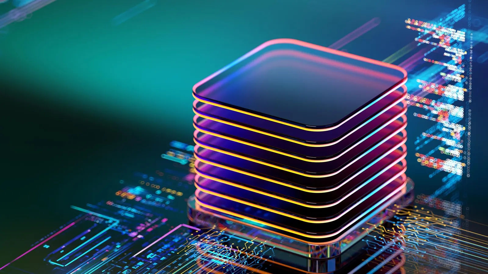
Chip stacking involves vertically integrating multiple semiconductor dies on top of one another.
Examples include:
- 3D Integrated Circuits (3D ICs)
- High Bandwidth Memory (HBM)
- 3D NAND Flash
- Logic-on-memory architectures
- Chiplet-based systems
This approach reduces communication distance between components and increases overall system density.
Why Traditional Scaling Is Slowing
For decades, semiconductor progress followed Moore's Law, where transistor density roughly doubled over time. However, modern chip manufacturing faces increasing challenges.
- Rising fabrication costs
- Thermal constraints
- Quantum-scale physics limitations
- Power density challenges
- Manufacturing complexity
Advanced packaging offers an alternative path for improving performance without relying solely on smaller transistors.
How Advanced Packaging Works
Advanced semiconductor systems integrate multiple dies using specialized interconnect technologies.
Typical workflow:
- Individual semiconductor dies are fabricated.
- Specialized chiplets are designed for different tasks.
- Interconnect structures are created.
- Components are stacked or integrated.
- Thermal and power systems are optimized.
- The complete package operates as a unified system.
The result is a modular and highly optimized computing architecture.
Major Advanced Packaging Technologies
- 2.5D Packaging
- 3D Chip Stacking
- Chiplet Architectures
- System-in-Package (SiP)
- Fan-Out Wafer-Level Packaging
- Through-Silicon Vias (TSVs)
- Hybrid Bonding
These technologies enable highly integrated semiconductor ecosystems.
Role in Artificial Intelligence
AI workloads require massive memory bandwidth and parallel processing capability.
- AI accelerators
- Large language models
- GPU clusters
- Neural network training
- Inference optimization
Advanced packaging allows processors and memory to operate much more efficiently together.
The future of semiconductor performance may depend less on shrinking transistors and more on how intelligently chips are interconnected and stacked.
Benefits of Advanced Packaging & Chip Stacking
- Higher computing performance
- Improved energy efficiency
- Reduced latency
- Greater bandwidth
- Smaller physical footprint
- Modular chip design flexibility
- Enhanced scalability
These advantages are increasingly important for next-generation computing systems.

Traditional Semiconductor Design vs Advanced Packaging
| Traditional Monolithic Chips | Advanced Packaging & Chip Stacking |
|---|---|
| Single large die | Multiple integrated chiplets |
| Horizontal scaling focus | Vertical + modular integration |
| Longer interconnect distances | Short high-speed interconnects |
| Limited flexibility | Customizable architectures |
Applications Across Industries
- Artificial Intelligence
- Data Centers
- Autonomous Vehicles
- Edge Computing
- Quantum Computing
- 5G and 6G Infrastructure
- Defense Electronics
Advanced packaging is becoming central to modern computing ecosystems.
Challenges and Risks
- Thermal management complexity
- Manufacturing challenges
- Yield optimization issues
- Higher packaging costs
- Design interoperability requirements
- Supply-chain dependencies
Successfully scaling advanced packaging requires major engineering and manufacturing innovation.
Role of AI in Packaging Design
Artificial intelligence is increasingly being used to optimize semiconductor packaging systems.
- Thermal simulation
- Interconnect optimization
- Manufacturing process control
- Defect detection
- Yield prediction
AI-assisted engineering may accelerate the next generation of chip integration technologies.
Future Outlook
The semiconductor industry is expected to increasingly embrace modular and vertically integrated architectures.
- AI-native processors
- Massive chiplet ecosystems
- Integrated photonics
- Embedded cooling systems
- Heterogeneous computing platforms
Future computing systems may consist of highly specialized stacked architectures optimized for specific workloads.
Economic and Strategic Implications
Advanced Packaging & Chip Stacking could redefine semiconductor competitiveness in the AI era.
- Expansion of advanced semiconductor markets
- Acceleration of AI infrastructure growth
- Enhanced national semiconductor capabilities
- Improved computing efficiency
- Creation of new chip ecosystem business models
The organizations and nations that master advanced integration technologies may shape the future of global computing infrastructure.
Frequently Asked Questions
What is Advanced Packaging?
Advanced packaging refers to semiconductor technologies that integrate multiple chips and components into highly optimized computing systems.
What is Chip Stacking?
Chip stacking is the vertical integration of multiple semiconductor dies to improve performance, density, and energy efficiency.
Why is advanced packaging important for AI?
AI systems require extremely high memory bandwidth, processing power, and energy efficiency, which advanced packaging technologies help provide.
Conclusion
Advanced Packaging & Chip Stacking represents one of the most important transitions in the evolution of semiconductor engineering. As traditional transistor scaling approaches become increasingly difficult, modular integration and vertical chip architectures are emerging as critical pathways for sustaining computing progress. By enabling more powerful, efficient, and scalable systems, advanced packaging technologies may define the next era of artificial intelligence, hyperscale infrastructure, and high-performance computing innovation.