AI Packaging in Advanced Semiconductor Manufacturing
The semiconductor industry is entering a transformative era driven by artificial intelligence, high-performance computing, edge intelligence, autonomous systems, and next-generation data centers. As AI models grow exponentially in complexity, traditional chip scaling approaches are reaching physical and economic limitations.
To overcome these challenges, the industry is increasingly focusing on advanced semiconductor packaging—the science of integrating multiple chips into highly optimized systems. Artificial intelligence is now becoming a critical component in designing, optimizing, manufacturing, and managing these advanced packaging technologies.
This convergence is giving rise to a new paradigm known as AI Packaging in Advanced Semiconductor Manufacturing, where AI systems help create more powerful, efficient, and scalable semiconductor architectures.
This evolution could fundamentally reshape computing performance, chip economics, and the future of digital infrastructure.

What Is Advanced Semiconductor Packaging?
Advanced packaging refers to techniques used to combine multiple semiconductor components into a unified high-performance system.
Examples include:
- 2.5D Packaging
- 3D Chip Stacking
- Chiplet Architectures
- Fan-Out Packaging
- Heterogeneous Integration
- System-in-Package (SiP)
Rather than relying solely on transistor miniaturization, advanced packaging improves performance through smarter integration.
Why Traditional Chip Scaling Is Slowing
For decades, semiconductor progress was driven by Moore's Law. However, physical and economic constraints are making continued transistor scaling increasingly difficult.
- Rising fabrication costs
- Thermal limitations
- Power consumption challenges
- Manufacturing complexity
- Yield constraints
Advanced packaging is emerging as a key pathway for future performance improvements.
What Role Does AI Play?
Artificial intelligence is increasingly used throughout the semiconductor packaging lifecycle.
- Package design optimization
- Thermal management analysis
- Manufacturing process control
- Defect detection
- Yield optimization
- Supply-chain forecasting
- Performance simulation
AI helps engineers solve problems that would be extremely difficult using traditional methods alone.
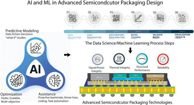
How AI Optimizes Chip Packaging
Modern packaging systems involve billions of variables affecting performance.
AI systems can analyze:
- Power distribution networks
- Signal integrity paths
- Heat dissipation patterns
- Interconnect placement
- Manufacturing tolerances
- Performance bottlenecks
This enables faster design cycles and improved outcomes.
Key Technologies Driving AI Packaging
- Machine Learning Algorithms
- Digital Twin Systems
- Computer Vision Inspection
- Generative Design AI
- Predictive Analytics Platforms
- EDA (Electronic Design Automation) Tools
- Physics-Informed AI Models
These technologies enable intelligent decision-making throughout the manufacturing process.
Applications Across the Semiconductor Industry
AI-driven packaging innovations are increasingly important for:
- AI Accelerators
- Data Center GPUs
- Smartphones
- Autonomous Vehicles
- Edge Computing Devices
- High-Performance Computing Systems
- Defense and Aerospace Electronics
Packaging innovation is becoming a competitive differentiator.
The future of semiconductor performance may depend less on shrinking transistors and more on how intelligently chips are packaged together.
Benefits of AI Packaging
- Improved chip performance
- Lower power consumption
- Higher manufacturing yields
- Reduced development costs
- Faster time-to-market
- Enhanced scalability
- Better thermal efficiency
AI helps maximize the value of increasingly complex semiconductor systems.

Traditional Manufacturing vs AI-Assisted Packaging
| Traditional Approach | AI-Assisted Approach |
|---|---|
| Manual optimization | Automated optimization |
| Long design cycles | Accelerated development |
| Reactive quality control | Predictive quality management |
| Limited simulations | Massive AI-driven simulations |
Challenges and Risks
- Complex implementation requirements
- Data quality limitations
- High infrastructure costs
- Cybersecurity concerns
- Talent shortages
- Integration complexity
Successful deployment requires collaboration between semiconductor engineers and AI specialists.
Future Outlook
The semiconductor industry is expected to increasingly embrace AI-native packaging workflows.
- Fully autonomous chip design systems
- AI-driven digital fabs
- Self-optimizing packaging architectures
- Advanced chiplet ecosystems
- Next-generation heterogeneous integration
AI may become a foundational layer of semiconductor innovation.
Economic and Strategic Implications
AI Packaging in Advanced Semiconductor Manufacturing could become one of the most important drivers of future computing competitiveness.
- Acceleration of AI infrastructure growth
- Improved national semiconductor capabilities
- Lower manufacturing costs
- Enhanced technological sovereignty
- Expansion of advanced packaging markets
The companies that master AI-assisted packaging may define the next era of semiconductor leadership.
Frequently Asked Questions
What is advanced semiconductor packaging?
It refers to technologies that integrate multiple chips into a single high-performance package to improve efficiency, speed, and functionality.
How does AI help semiconductor manufacturing?
AI assists with design optimization, defect detection, yield improvement, thermal analysis, and manufacturing automation.
Why is packaging becoming more important?
As transistor scaling slows, advanced packaging provides a new way to improve performance and efficiency through better chip integration.
Conclusion
Manufacturing represents the convergence of artificial intelligence and next-generation chip engineering. As the limits of traditional scaling become more apparent, intelligent packaging solutions offer a powerful path forward. By optimizing design, manufacturing, and system integration, AI is helping create the semiconductor architectures that will power the future of computing, artificial intelligence, and digital transformation.